Recently, the ultra-precision surface manufacturing team of the Institute of Tribology of the School of Mechanical Engineering, with Southwest Jiaotong University as the first corresponding affiliation, cooperated with the State Key Laboratory of Tribology of Tsinghua University and wrote a report on the semiconductor in Nature Communications. Research progress in the ultimate processing of wafer materials has enabled the controlled removal of single-layer silicon atoms. This is the first paper published in this Journal led by Southwest Jiaotong University. The first author of the paper is Lei Chen, associate researcher of the School of Mechanical Engineering. The co-corresponding author is Professor Linmao Qian of the School of Mechanical Engineering and Professor Xinchun Lu of the State Key Laboratory of Tribology of Tsinghua University.
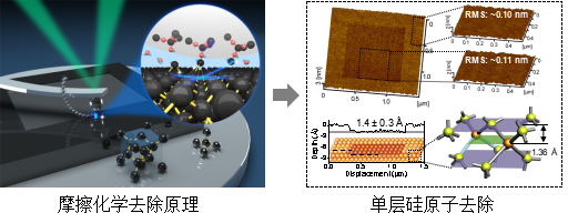
The realization of ultrafine manufacturing with atomic precision is very important to the development of the unique functions of nano-electronic devices in the nano-machining process. The ultra-precision surface manufacturing team cooperated with the State Key Laboratory of Tribology of Tsinghua University to realize the extreme precision machining of monocrystalline silicon material surface without layered cleavage surface based on the scanning probe technology for the first time, namely the controllable removal of monocrystalline silicon atoms. This method does not require a mask, no chemical corrosion, can be directly processed by friction chemical reaction in the ordinary humid environment.
Unlike the wear, fracture and plastic deformation of materials in traditional machining, the tribochemical removal of monocrystalline silicon atomic materials is mainly attributed to the stripping of the silicon atoms in the matrix under the atomic bonding between the sliding interfaces. Therefore, the subsurface crystal structure after the removal of the atomic layered material remains intact and no defects such as slip or lattice distortion are generated. This study gives direct evidence for the atomic layer removal of single crystal silicon materials by high-resolution transmission electron microscopy. Combined with molecular dynamics simulation, it reveals the tribochemical peeling mechanism of silicon atoms and the ultimate precision processing of semiconductor wafer materials. It has also made greatly progress in the study of limiting precision fabrication of semiconductor wafer materials..
The research was supported by projects such as the National Natural Science Foundation of China and the Major Nanotechnology Research Program.
(full text link: https://rdcu.be/LSkz)